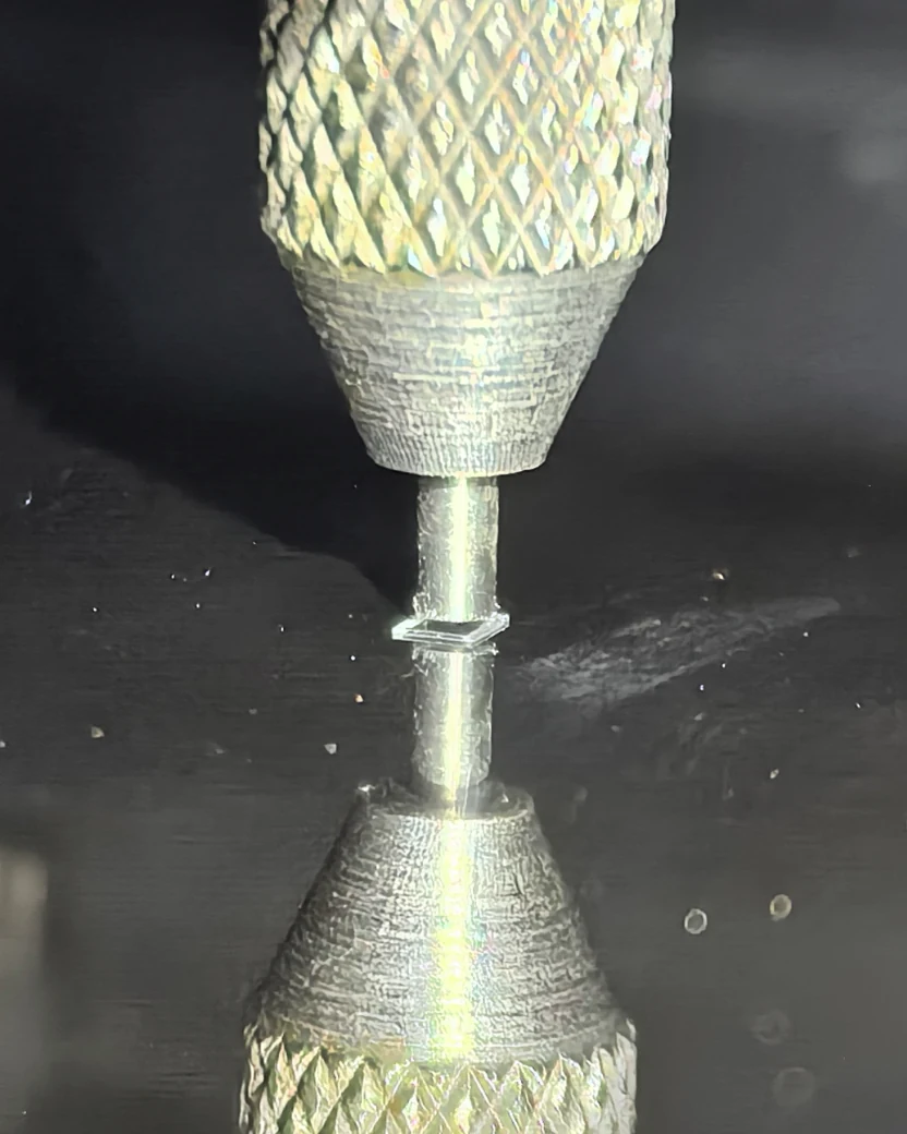
A process and R&D analysis instrument that handles a whole wafer or a single die: blank and etched wafers, coated wafers depending on the film and electrode contact, plus singulated flat dies and loose MESA after dicing. CCD vision locates the wafer frame and measures each die centre in turn; the probe gap closes automatically at micron resolution, and results export straight to Excel.
More below — specs & details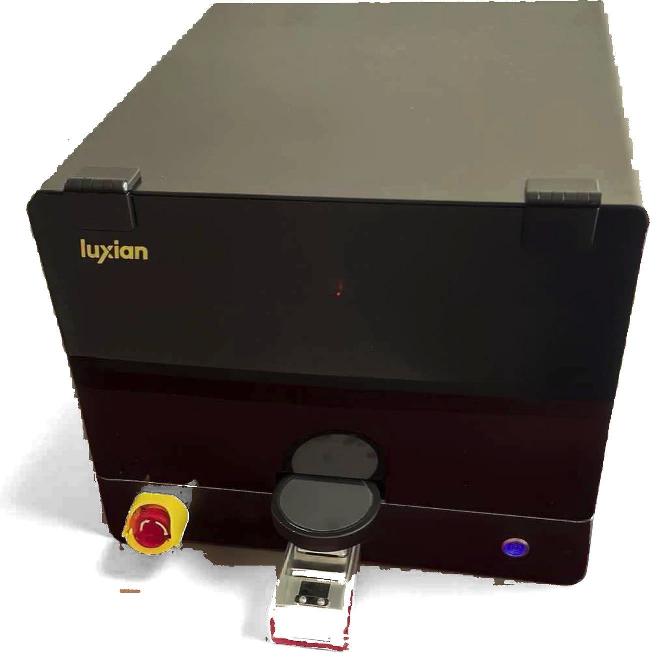
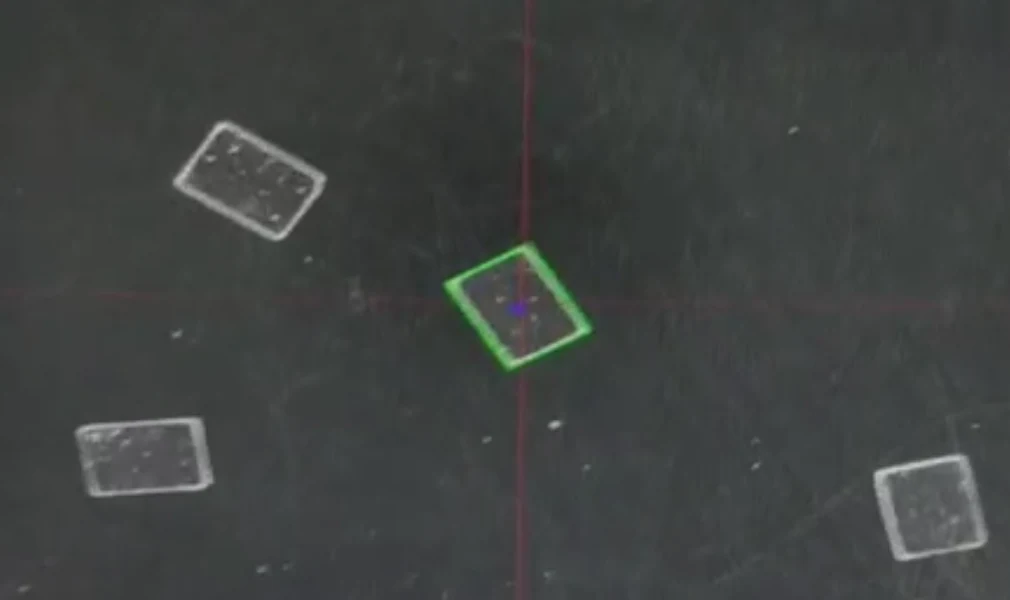
CCD finds the frame, then locates and measures every die.
Recognises the MESA structure separately to remove off-centre error.
0.002 mm zeroing repeatability, no operator variance.
Define test points in Excel; reports come out automatically.
Floor 2, Building C, Space Big Data Park, No. 20 Kangyuan Road, Xuanwu District, Nanjing, China
Mon–Sat, 8:30–17:00 (GMT+8)