禄宪 luxian
中 / EN
Home/ Products/ QB-WT-200
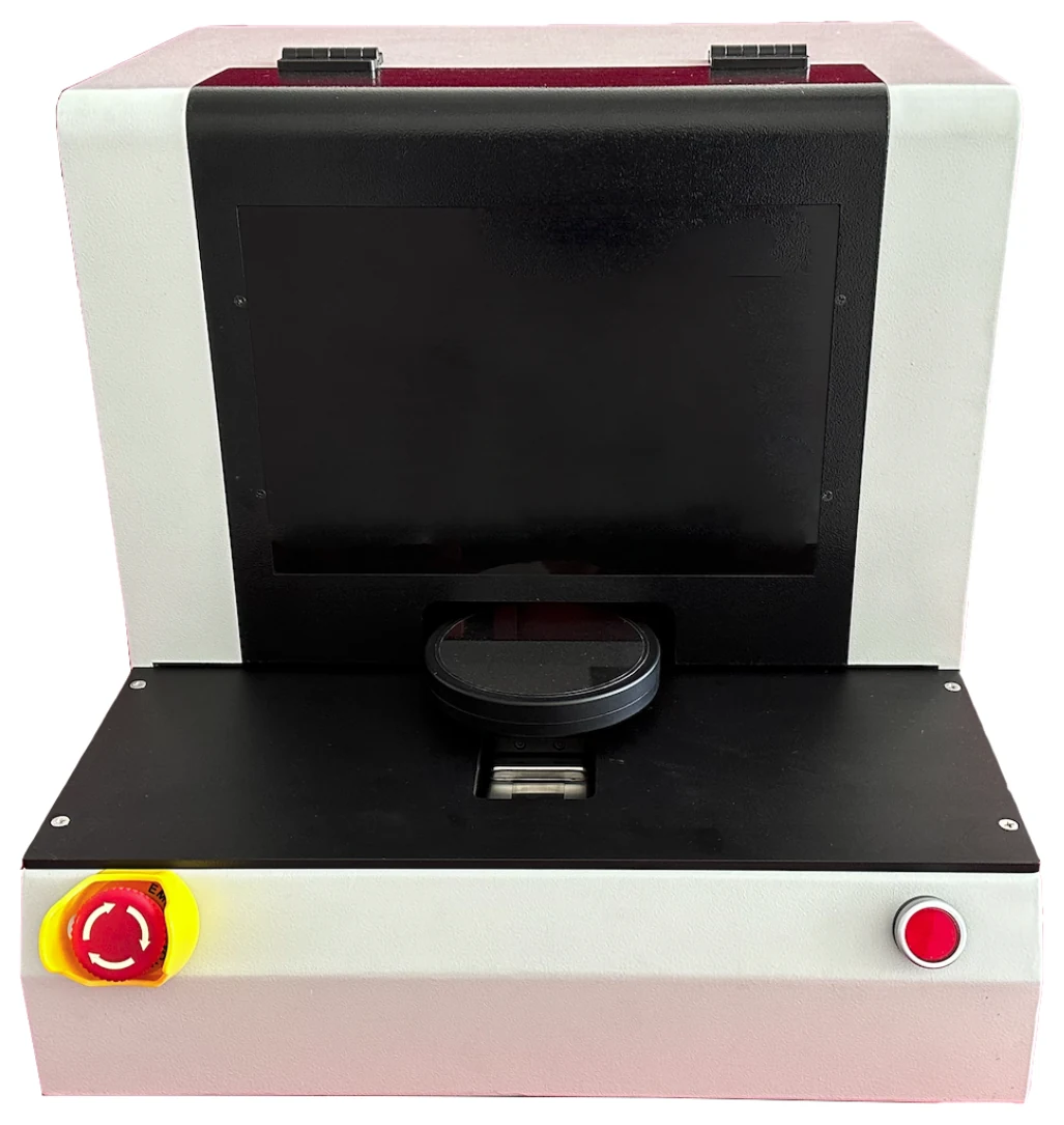
QB-WT-200

Quartz Wafer Surface Analyzer

Thickness from frequency, map and 3D

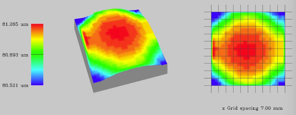
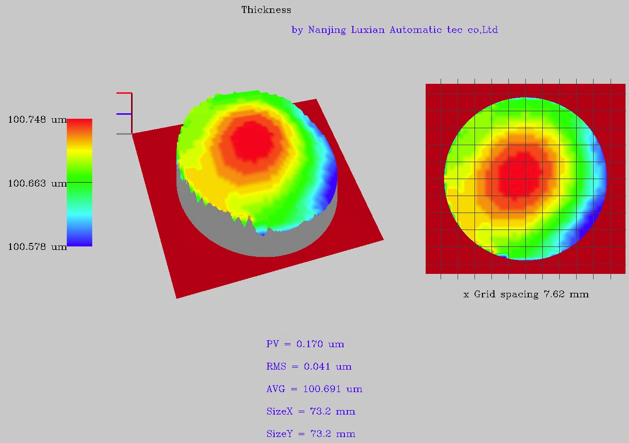
A process analysis instrument for surface-profile mapping through development and small-volume production. CCD locates the wafer frame, thickness is derived from the frequency measured at each point, and the result comes out as an Excel report, a colour map and a 3D surface.

More below — specs & details
QB-WT-200

2 / 3 / 4 inch wafers

Square wafers up to 100 mm diagonal as well.

Frequency to thickness

Point-by-point measurement mapped to thickness.

0.003 μm flip-side agreement

Re-measured with the wafer flipped: 0.003 μm on average and RMS, 0.01 μm PV.

Map, 3D and Excel

PV, RMS, AVG, SizeX/Y reported directly.
Specifications

Specifications

Samples
2, 3, 4 inch round wafers; square wafers under 100 mm diagonal
Method
CCD frame recognition, auto positioning, robotic test
Principle
Frequency measured per point, thickness derived
Frequency source
Luxian network analyzer, 2–200 MHz
Surface metrics
PV, RMS, AVG, SizeX / SizeY
Repeatability
Same wafer, flipped: 0.003 μm mean, 0.003 μm RMS, 0.01 μm PV
Output
Excel report, colour map, 3D surface
Environment
25±5 °C, 55–75% RH
Details

Details & output

Related

Related equipment

Contact

Need help choosing?

Floor 2, Building C, Space Big Data Park, No. 20 Kangyuan Road, Xuanwu District, Nanjing, China
Mon–Sat, 8:30–17:00 (GMT+8)

Tel
Mr. Huang
13951899360
Tel
Mr. Ji
13851695621

Contact us →