A custom-configured process analysis system for lithography wafers, from development through small-volume production. It handles blank wafers before etching, etched and coated wafers, singulated dies and loose MESA. Image processing locates each sub-die; a high-precision 4-axis robot holds repeatable positioning.
More below — specs & details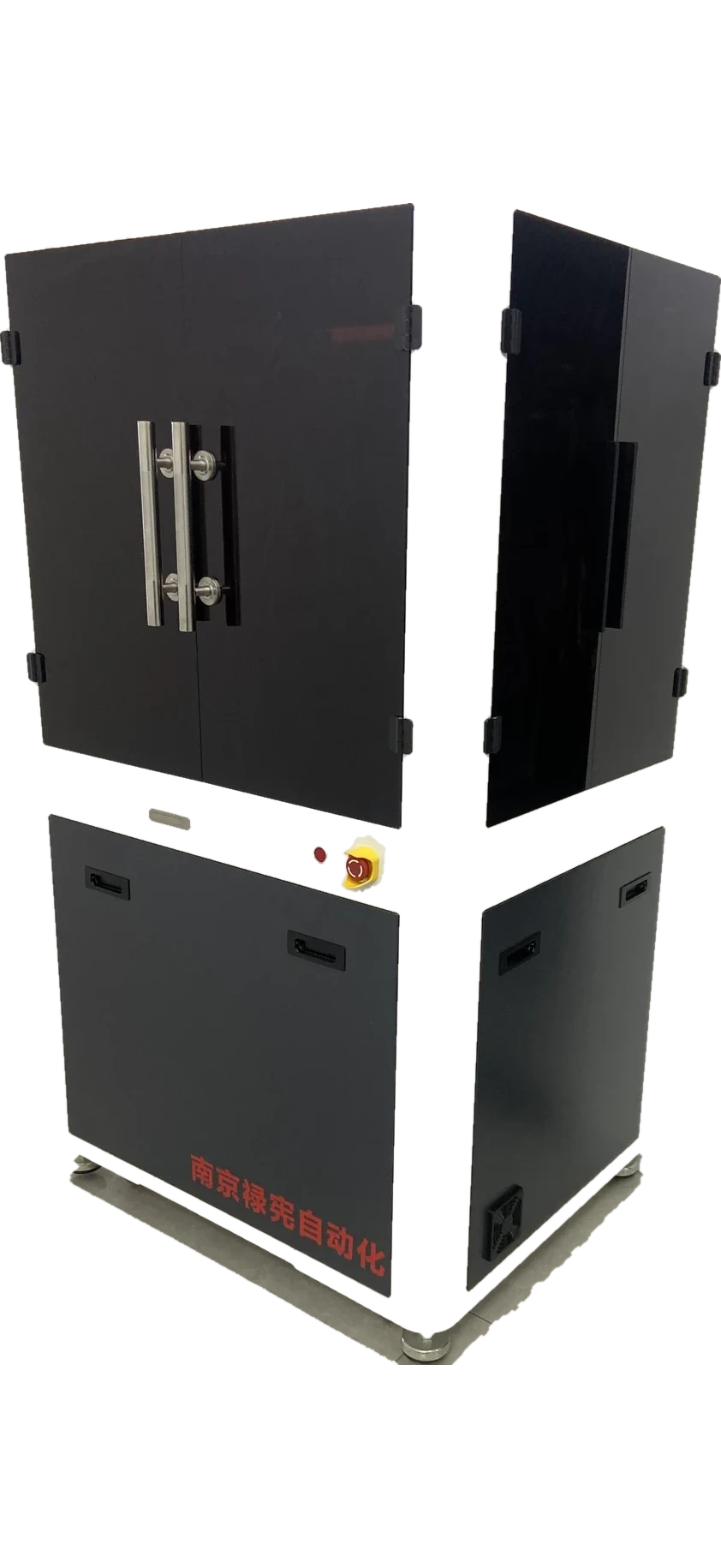
Image processing finds and locates them.
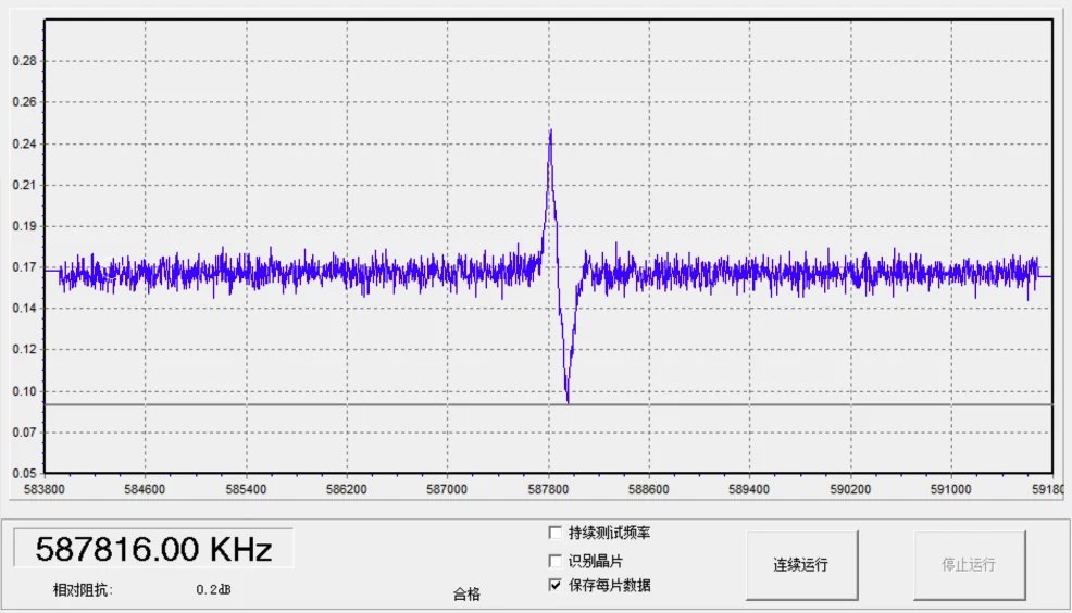
Optimised for contact-free and very high frequency dies.
Repeatable positioning, with point verification.
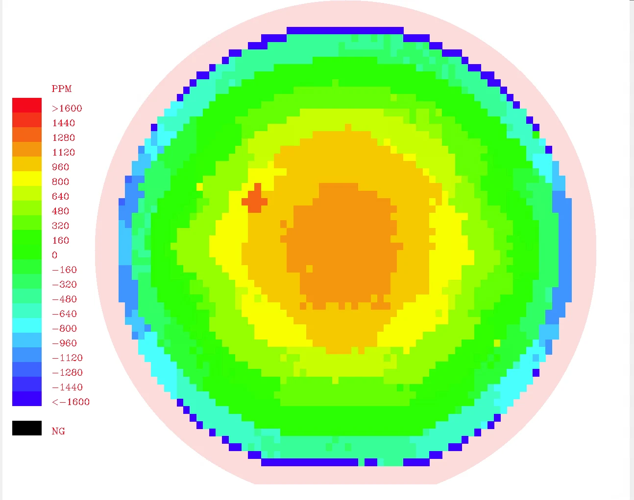
Sub-die map and Excel report, fully traceable.
Floor 2, Building C, Space Big Data Park, No. 20 Kangyuan Road, Xuanwu District, Nanjing, China
Mon–Sat, 8:30–17:00 (GMT+8)